News
New Publication “PHz Electronic Device Design and Simulation for Waveguide-Integrated Carrier-Envelope Phase Detection”
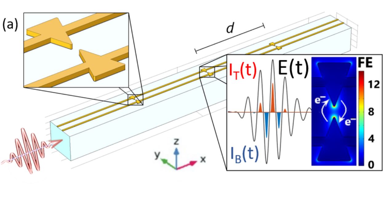
Carrier-envelope phase (CEP) detection of ultrashort optical pulses and low-energy waveform field sampling have recently been demonstrated using direct time-domain methods that exploit optical-field photoemission from plasmonic nanoantennas. These devices are compact and integratable solid-state detectors operating at optical frequencies under ambient conditions using low pulse energies (picojoule-level). Potential applications include frequency-comb stabilization, optical time-domain spectroscopy, compact tools for attosecond science and metrology, and petahertz-scale information processing. However, to date these devices have been driven by free-space optical waveforms and their implementation within integrated photonic platforms has yet to be demonstrated. In this work, we design and simulate fully-integrated plasmonic nanoantennas coupled to a SiN-core waveguide for CEP detection. We find that when coupled to realistic on-chip, few-cycle supercontinuum sources, these devices are suitable for direct time-domain CEP detection within integrated photonic platforms. We estimate a signal-to-noise ratio of 30 dB at 50 kHz resolution bandwidth, and address technical details, such as the tuning of the nanoantennas plasmonic resonance, CEP slippage in the waveguide, optical losses, and sensitivity to driving pulse characteristics such as energy and duration. Our results provide the basis for future design and fabrication of time-domain CEP detectors and allow for the development of fully-integrated attosecond science applications, frequency-comb stabilization and light-wave-based PHz electronics.
A complete description of the work may be found here.
QNN Quarterly Newsletter
We’ve had a busy summer in the lab and in terms of sharing our results. Here are a number of published papers and key activities.
Comings and Goings
This summer we welcomed the following new group members:
- Kate Artyunova, UROP
- Matteo Castellani, EECS Grad Student
- Andrew Sorenson, MEng Grad Student
The following members have now left and become alumni group members:
- Akshay Agarwal, completed his PhD!
- Thesis title “Techniques for Enhancing Electron Microscopy”
- Tao Cai, Summer UROP returning to University of Michigan
- Dario Cattozzo Mor, Junior Researcher at Czech Academy of Sciences
- Andres Lombo, returning to Senior year at University of Toronto
- Glenn Martinez, Successfully defended his MS Thesis!
- Di Zhu, taking technical staff position at IMRE in Singapore
Awards
- Marco Colangelo – Claude E. Shannon Award
Publications
[1] X. Zhang et al., “Physical properties of amorphous molybdenum silicide films for single-photon detectors,” Supercond. Sci. Technol., vol. 34, no. 9, p. 095003, Aug. 2021, doi:10.1088/1361-6668/ac1524.
[2] Q. Xie et al., “NbN-Gated GaN Transistor Technology for Applications in Quantum Computing Systems,” in 2021 Symposium on VLSI Technology, Jun. 2021, pp. 1–2.
[3] J. W. Simonaitis, B. Slayton, Y. Yang-Keathley, P. D. Keathley, and K. K. Berggren, “Precise, subnanosecond, and high-voltage switching enabled by gallium nitride electronics integrated into complex loads,” Review of Scientific Instruments, vol. 92, no. 7, p. 074704, Jul. 2021, doi:10.1063/5.0046706.
[4] D. Buckley, Y. Yang, Y. Yang-Keathley, K. K. Berggren, and P. D. Keathley, “Nanoantenna design for enhanced carrier–envelope-phase sensitivity,” J. Opt. Soc. Am. B, JOSAB, vol. 38, no. 9, pp. C11–C21, Sep. 2021, doi:10.1364/JOSAB.424549.
[5] M. R. Bionta et al., “On-chip sampling of optical fields with attosecond resolution,” Nat. Photonics, vol. 15, no. 6, pp. 456–460, Jun. 2021, doi:10.1038/s41566-021-00792-0.
[6] M. R. Bionta et al., “Tracking ultrafast solid-state dynamics using high harmonic spectroscopy,” Phys. Rev. Research, vol. 3, no. 2, p. 023250, Jun. 2021, doi:10.1103/PhysRevResearch.3.023250.
[7] R. Bhattacharya, M. Turchetti, P. D. Keathley, K. K. Berggren, and J. Browning, “Long term field emission current stability characterization of planar field emitter devices,” Journal of Vacuum Science & Technology B, vol. 39, no. 5, p. 053201, Sep. 2021, doi:10.1116/6.0001182.
[8] N. Abedzadeh et al., “Electrostatic electron mirror in SEM for simultaneous imaging of top and bottom surfaces of a sample,” Ultramicroscopy, vol. 226, p. 113304, Jul. 2021, doi:10.1016/j.ultramic.2021.113304.
Talks
CLEO2021
M. Colangelo et al., “Impedance-matched differential SNSPDs for practical photon counting with sub-10 ps timing jitter,” in Conference on Lasers and Electro-Optics (2021), May 2021, p. FW2P.1. doi:10.1364/CLEO_QELS.2021.FW2P.1.
M. Cattozzo Mor et al., “PHz Electronic Device Design for Waveguide-Integrated Carrier-Envelope Phase Detection,” in Conference on Lasers and Electro-Optics (2021), paper SW3J.3, May 2021, p. SW3J.3. doi:10.1364/CLEO_SI.2021.SW3J.3.
Lund Attosecond Symposium 2021
M. R. Bionta, “Tracking solid-state phase transitions with time-resolved HHG spectroscopy,” presented at the Lund Attoscience Symposium 2021, Virtual, Jun. 16, 2021.
IVNC2021
M. Turchetti, “Emission Behavior of Planar Nano-Vacuum Field Emitters,” presented at the 34th International Vacuum Nanoelectronics Conference, Virtual, Jul. 07, 2021. [Online].
LTD19
T. X. Zhou, “Ultra-wide MoSi SNSPD detectors,” presented at the 19th International Workshop on Low Temperature Detectors (LTD19), Virtual, Jul. 29, 2021. [Online].
ICN+T
P. D. Keathley, “On-Chip Petahertz Processing of Optical Fields,” presented at the ICN+T, Virtual, Jul. 2021.
Patents
Submission: US 63/076,463 Marco Turchetti, Mina R. Bionta, Felix Ritzkowsky, , Yujia Yang, Dario Cattozzo Mor, William P. Putnam, Franz X. Kärtner, Karl K. Berggren, Phillip D. Keathley “Integrated Optical Field Sampling Platform”
New Publication “Physical properties of amorphous molybdenum silicide films for single-photon detectors”
We systematically investigated the physical properties of amorphous MoxSi1−x films deposited by magnetron co-sputtering. The critical temperature Tc of MoxSi1−x films increases gradually with the Mo stoichiometry x, and the highest Tc = 7.9 K was found in Mo0.83Si0.17, where homogeneous films with the maximum Mo content can be obtained. The thick films of Mo0.83Si0.17 show surprising degradation in which the onset of zero-resistivity is suppressed below 2 K. The thin Mo0.83Si0.17films, however, reveal robust superconductivity even with thickness d ≈ 2 nm. We also characterized wide microwires based on the 2 nm thin Mo0.8Si0.2 films with wire widths 40 and 60 μm, which show single-photon sensitivity at 780 nm and 1550 nm wavelength.
A complete description of the work may be found here.
Talks at CLEO2021 Conference
Our group participated in the CLEO2021 conference with two talks. You can find the abstracts at the following links:
- Marco Colangelo – Impedance-matched differential SNSPDs for practical photon counting with sub-10 ps timing jitter
- Dario Cattozzo Mor – PHz Electronic Device Design for Waveguide-Integrated Carrier-Envelope Phase Detection
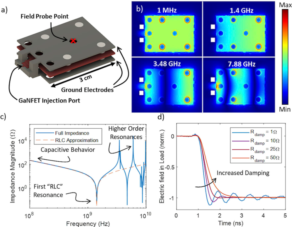
New Publication “Precise, subnanosecond, and high-voltage switching enabled by gallium nitride electronics integrated into complex loads”
In this work, we report the use of commercial gallium nitride (GaN) power electronics to precisely switch complex distributed loads, such as electron lenses and deflectors. This was accomplished by taking advantage of the small form-factor, low-power dissipation, and high temperature compatibility of GaN field effect transistors (GaNFETs) to integrate pulsers directly into the loads to be switched, even under vacuum. This integration reduces parasitics to allow for faster switching and removes the requirement to impedance match the load to a transmission line by allowing for a lumped element approximation of the load even with subnanosecond switching. Depending on the chosen GaNFET and driver, these GaN pulsers are capable of generating pulses ranging from 100 to 650 V and 5 to 60 A in 0.25–8 ns using simple designs with easy control, few-nanosecond propagation delays, and MHz repetition rates. We experimentally demonstrate a simple 250 ps, 100 V pulser measured by using a directly coupled 2 GHz oscilloscope. By introducing resistive dampening, we can eliminate ringing to allow for precise 100 V transitions that complete a −10 to −90 V transition in 1.5 ns, limited primarily by the inductance of the oscilloscope measurement path. The performance of the pulser attached to various load structures is simulated, demonstrating the possibility of even faster switching of internal fields in these loads. We test these circuits under vacuum and up to 120 °C to demonstrate their flexibility. We expect these GaN pulsers to have broad application in fields such as optics, nuclear sciences, charged particle optics, and atomic physics that require nanosecond, high-voltage transitions.
A complete description of the work may be found here.